Ring PCB Technology Co.,Limited
Our market is the Multilayer PCB(40L), HDI PCB(2 steps), Special process & Special material PCB, such as Aluminum base PCB, Rigid-Flex PCB, High-Frequency PCB, Heavy Copper PCB ( 19OZ ), and so on.
Multi-layer PCB
Multilayer PCB Manufacturing
The manufacture of high-layer, high-difficulty, special materials, special process circuit boards, which has always been our characteristics; the continuous improvement of high-multi-layer circuit board manufacturing process as our goal. Every year we invest a lot of human resources and material resources in production equipment and process research and development and try our best to catch up with the development of cutting-edge circuit board manufacturing technology.
PCB Process Capabilit
Multilayer Printed Circuit Board
We can produce up to 40 layers of high-layer circuit boards, various buried and blind vias circuit boards, and HID PCB. HDI PCB can be up to 2 steps.
High-difficult PCB
①: Min hole we can drill is 0.15mm, and 0.075mm for HDI design, and high-density print circuit board. ②: We can control impedance both single-end and differential for multi-layer(the min trace width/space is 4mil/4mil) ③: High precision circuit board( min trace width we can do 3mil, and the thinnest core we can do is 0.05mm) ④: Other special material board
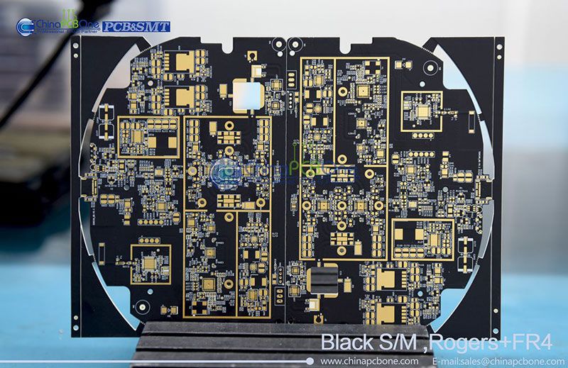
Heavy copper board( copper weight:210-700um), copper base material, aluminum, PI material, BT material, high-frequency material, Rogers Series, PTFE material, Taconic Series, Arlon.
Special Material
Special Technology
①: Flex-rigid board, high to six layer flex in the inner layer, gold finger in flex area. ②: Steps boards: can expose the pad and circuit for inner circuit ③: Mixture surface treatment: OSP+ENIG ④: Multi-layer metal board: double side copper baseboard, double side aluminum board. ⑤: Mixture laminating: can process two or more material mixture laminating, like Ceramic +FR4+PTFE ⑥: Multi-frequency board: every board use high-frequency material ⑦: Plugging resin
Processing high quality is the essential requirement for every staff
①: We strictly train and test the operation for staff
②: The quality department will check every status for all the board, to ensure the board can meet the quality requirement.
③: Providing all test equipment( like AOI, fly probe machine and all kinds of test machine), so that can ensure and improve the quality checking.
High-Quality Insurance
Including Electronic consumption, Industrial manufacturing, LED lighting, electric power, Bluetooth communication, Radar antenna, aviation, automobile, and high-frequency communication.
all kinds of industrial
The Application for Multi-layer PCB
Special Material for PCB
Normal FR4, high TG FR4, PTFE, ceramic, aluminum, metal base, flex material, BT, PI, and so on.
all kinds of material
Include FR4+ceramic laminating, PTFE+FR4 laminating, heavy copper, flex-rigid, multi-layer, and impedance control. Also, we can process blind& buried hole, via in pad, plugging resin and countersink, and so on special process. Besides, we can process step boards with professional experience.
all kind of process
Special Process for PcB


