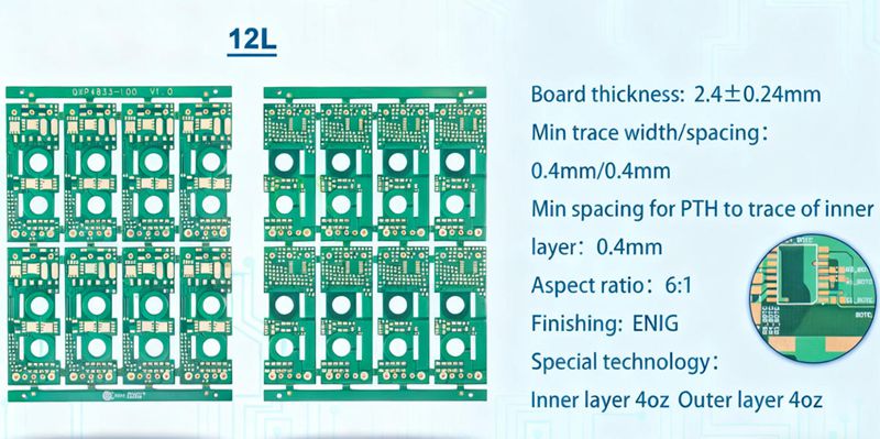
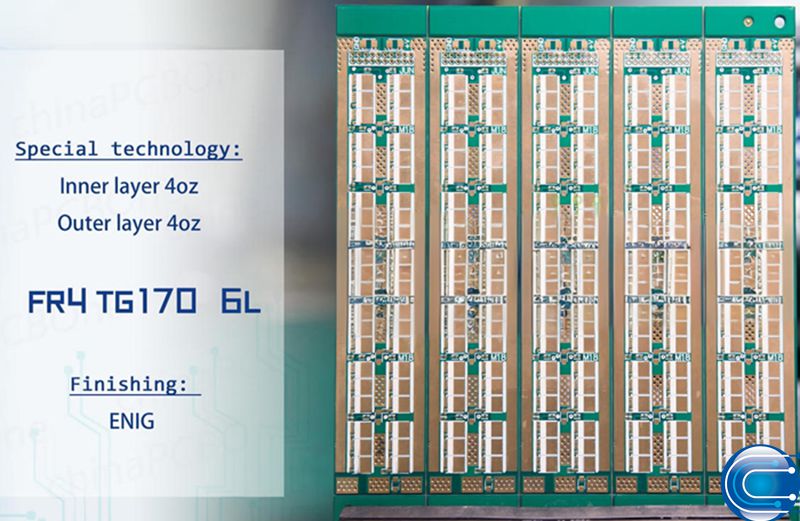
Since 2008, Ring PCB has specialized in the design and manufacturing of Heavy Copper PCBs at our advanced factory in Shenzhen, China. With over a decade of experience, we deliver robust, high-quality Heavy Copper PCBs tailored for demanding applications in industries such as automotive, aerospace, military, power distribution, and renewable energy.
What Are Heavy Copper PCBs?
Heavy copper PCBs are also known as thick copper PCBs or power PCBs. They are unique due to their significantly thicker copper layers—typically ranging from 3 oz/ft² up to 20 oz/ft² or more. Standard PCBs typically have copper thicknesses of less than 2 oz/ft², so the enhanced current-carrying capacity of Heavy Copper PCBs makes them suitable for high-power applications.
How to Achieve a Thick Copper?
1.Initial Base Material: There are base materials with thicker copper foils (e.g., 6 oz copper thickness laminates), but generally we prefer to use standard copper laminates and build up the copper thickness, because thick copper laminates are more expensive than standard copper laminates.
2.Electroplating Process: The PCB is immersed in a copper sulfate solution where an electric current is applied to deposit copper onto the exposed areas. The plating process is controlled to deposit additional copper where it's needed, especially on thicker power or ground planes, vias, and pads. This is where the copper thickness can be significantly increased to the desired level.
3.Multiple Plating Steps: In some cases, multiple electroplating steps are used to build up the copper layer to the required thickness, ensuring uniformity in vias, traces, and pads.
The Manufacturing Challenges for Heavy Copper PCBs at Ring PCB
1. Etching Process
Challenge: Standard PCB etching techniques struggle with thick copper layers. As copper thickness increases, the etching process becomes more difficult, requiring precise control to avoid uneven or incomplete etching.
Solution: Advanced etching processes are employed to handle thicker copper, using controlled chemical etching and temperature management to achieve uniform copper traces. In some cases, multiple etching steps are used to gradually achieve the desired thickness.
2. Thermal Management During Manufacturing
Challenge: Thick copper layers retain heat, which can lead to issues with warping, delamination, or internal stress during high-temperature processes like lamination and soldering.
Solution: Temperature control and gradual thermal cycling are applied throughout manufacturing. Special solder masks that can endure higher temperatures are also used to prevent damage during soldering and reflow.
3.Drilling and Hole Quality
Challenge: Heavy Copper PCBs are more difficult to drill accurately due to their dense copper layers, which can cause bit wear, misalignment, and burrs around drilled holes.
Solution: Ring PCB reduces lifespan of drill bits and replace them sooner. Additionally, using high-precision drilling machines and specialized drill bits designed for thick copper can be beneficial. Furthermore, segmenting the drilling process can help minimize drill bit wear.
4.Copper Plating
Challenge: Plating thick copper requires copper plating layer can adhere to the original copper layer, enhancing the overall bonding strength.
Solution: PCBs are typically subjected to cleaning to remove contaminants, followed by both chemical and mechanical roughening to create a microscopically rough surface on the copper. A final copper plating step ensures uniform coverage.
5.Hole Size Compensation
Challenge: After the copper plating in Heavy Copper PCB manufacturing, the hole size can become smaller. This is because the plating process deposits additional copper within the drilled holes, increasing the thickness of the copper on the hole walls and slightly reducing the diameter.
Solution: Ring PCB carefully calculates the initial drill size based on the thickness of copper that will be added in the plating process. The hole is drilled slightly larger than the final required size to allow for the subsequent plating buildup.
6.Maintaining Trace Width and Spacing
Challenge: As copper thickness increases, controlling the trace width and spacing to achieve consistent conductivity and impedance becomes more challenging, especially with fine-line designs.
Solution: Ring PCB optimizes design rules to account for copper thickness. Laser imaging and high-precision exposure techniques ensure that traces are correctly formed, maintaining both electrical integrity and consistent layout.
Applications of Heavy Copper PCBs
Heavy Copper PCBs are indispensable in applications where high current and enhanced thermal performance are essential. Some common applications include:
Automotive Electronics: Used in electric vehicles, power converters, and braking systems due to their high current handling.
Aerospace and Military Equipment: Essential for equipment where reliability and durability in extreme environments are required.
Power Supplies: Heavy Copper PCBs are ideal for uninterruptible power supplies (UPS) and other high-power devices that require stable power management.
Renewable Energy: Found in wind turbines and solar power systems, where high current capacity and durability are needed for efficient energy conversion.
Industrial Equipment: Used in heavy-duty machinery, motor controls, and power distribution units for efficient heat management and reliability.
Ring PCB's Manufacturing Capabilities for Heavy Copper PCBs
Manufacturing Capability | Specification |
Copper Thickness | Up to 20 oz/ft² (700 μm) |
Layer Count | 2 to 20 layers |
Board Thickness | 0.5 mm to 5 mm |
Min. Trace Width/Spacing | 0.2 mm / 0.2 mm (may vary based on copper weight) |
Min. Hole Size | 0.25 mm (10 mil) |
Drilling Tolerance | ±0.05 mm |
Copper Plating in Through Holes | 25 μm to 75 μm |
Thermal Management | Embedded heatsinks, thermal vias |
Surface Finishes | ENIG, HASL, OSP, Immersion Tin, Immersion Silver |
Testing and Inspection | Automated Optical Inspection (AOI), X-ray inspection |
Solder Mask Types | High-temperature solder masks, peelable masks |
Vias Options | Plated through-holes, via-in-pad, buried, and blind vias |
Impedance Control | Available on request |
Standards Compliance | IPC-A-600, IPC-6012, RoHS compliant |
Why Choose Ring PCB for Heavy Copper PCBs?
Years of Expertise: With 17 years of experience in Heavy Copper PCB manufacturing, Ring PCB has a proven track record of producing reliable, high-quality products.
Advanced Machinery: Our factory in Shenzhen is equipped with state-of-the-art machinery, ensuring precision manufacturing and a high degree of quality control.
Industries We Serve: Whether you’re in automotive, aerospace, or industrial manufacturing, Ring PCB offers the quality and expertise to power your projects forward.


